

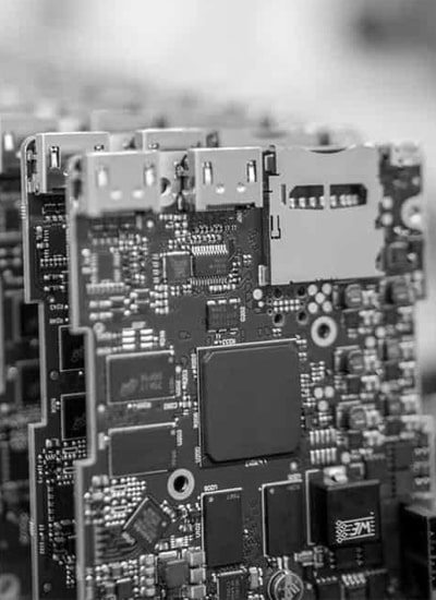
In this part of Pulse Tech articles, we will introduce various methods of making printed circuit boards.
There are several ways to make a printed circuit board or PCB, and you should choose one of them based on the complexity of the desired printed circuit and the facilities you have. Most of these methods are different in creating designs on fibers, but they can be divided into the following main methods.
Building a circuit with Letrast
Making a printed circuit with anti-acid ink
Printed circuit using laser and iron printing
Construction of the circuit with Purity spray
Circuit making with laser printing and laminator machine
Printed circuit production with laminate and UV
Circuit making with CNC
The most common manufacturing method for beginners is laser and iron printing, which is both easy and does not require many facilities. This method is often used to teach students and is not suitable for mass production. Anti-acid and letterpress magic methods are also very basic and are only useful for getting to know the technique and tools, and they are used in educational printed circuit kits because they are not very accurate. It can even be said that the positive spray method is one of the basic methods that are suggested to students and are more accurate than the previous methods.
In more professional printed circuit boards, laminate and UV are used, or mechanical and laser CNCs are used because it is both more accurate and more cost-effective in large-scale and high-volume productions.
As mentioned, different methods are used to make the printed circuit board, and you can consider the difficulty or ease of each of these methods, the available facilities, and the level of expectation from the quality level of the resulting printed circuit board. Choose one of them.
.
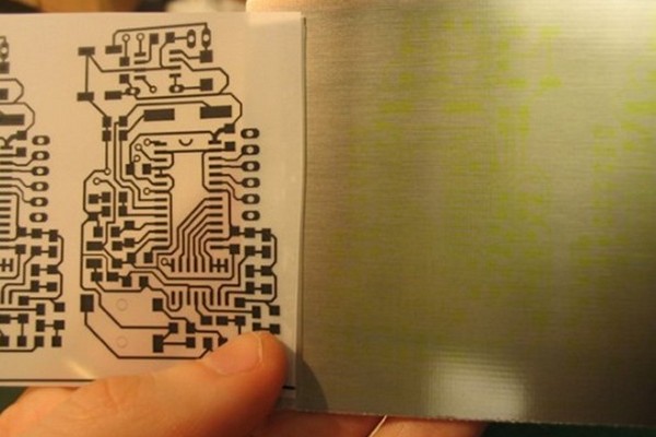
Familiarity with different methods of making printed circuit board
In this section of the Pulse Tech website, we are going to introduce some methods of making a printed circuit board.
• Using laser and iron printing
• Using letter trust method
• By using CNC machine
• By using anti-acid magic
• Using lamination method and UV rays
• Using laser printing and heating device
• By using Positive 20 spray
Making a printed circuit board with anti-acid ink
This simple method is usually used by novices and at the beginner level, and the resulting board will not be very clean and accurate. In this method, anti-acid ink and printed circuit acid are needed and it takes a lot of time. In addition, the quality of the resulting printed circuit board can be different depending on the materials used. This method is not considered a good option for medium and mass board production. We will explain the steps of making a printed circuit board with this method.
1- First, clean the copper fiber with the help of a soft sandpaper or in any other way and make sure that there is no layer of fat or dirt on the copper.
2- Then draw all the required lines on the copper fiber with the help of a colorful anti-acid marker that is special for this work. Because there is a possibility of losing the magic color if it is of poor quality, in water and acid, after designing and spending a lot of effort.
3- Remember to avoid touching the copper fiber due to its oiliness, because it can cause problems during the acidification stage.
4- You can use the stencil to create realistic sizes for parts such as ICs whose bases are approximately one-tenth of an inch apart, and by placing it on the copper, trace around it with a special marker that is sharp. draw With this method, you will be able to implement your entire design on fiber.
5- After completing the printed circuit board design, you can remove the excess parts of copper by placing the fiber in the acid.
.
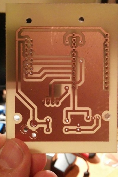
Making a printed circuit board with anti-acid ink
Making a printed circuit board using Letrast
This method, like the previous method of making a printed circuit board, is mostly used by beginners and the result will not be very accurate and clean. This method requires materials such as printing circuit acid and laterat. Letter trust is the same as the letters on the back, except that the dots and circular lines have replaced the letters on it. First, prepare some point and line letter trusts based on the type of circuit and your diagnosis. In order not to face any problem when returning it to the copper fiber, be sure to use fresh Letrast.
The steps of making a printed circuit board
In the rest of this section, we are going to introduce the steps of making a printed circuit board in this way:
1- First, in order to remove any grease and dirt on the copper, you must completely clean the copper fiber with a soft sandpaper or any other method.
2- After that, proceed to draw the required lines with letrast on copper. You can use the tip of a pen or another similar device to reverse the dots and lines on the copper. Don’t forget to avoid touching the copper in order to prevent the copper from becoming greasy and not to disturb the acid step.
3- Finally, make sure that the dots and lines on the copper stick completely, and if any of them do not stick, stick them to the copper surface with the help of a hair dryer and heating. It is even possible to use an anti-acid marker to fill in the spots that are not well covered with letterpress.
.
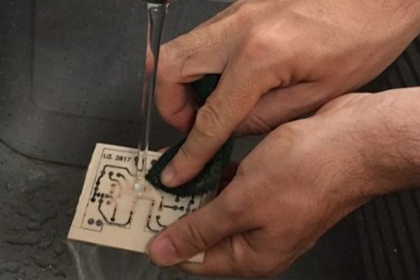
Making a printed circuit board using Letrast
4- In the next step and after completing the circuit, put it in acid to remove the excess parts of copper.
The method of making a printed circuit using laser and iron printing
In this method of making printed circuit board, materials such as suitable glossy paper, laser printer, as well as printed circuit acid and iron are used.
Making a printed circuit board with the help of this method is as follows:
1- Although liquid ink is used instead of toner in inkjet printers, the powder in the laser printer cartridge or the toner is made of plastic, and this printer uses powder by sprinkling the powder on the paper and registering the toner with the help of the resulting heat. From the laser, it performs the act of printing. During printing, the toner will be transferred to the paper in the form of powder after leaving the cartridge. Since copper fibers are hard, you will not be able to use the printer directly to create lines and other marks on the printed circuit board. So you have to transfer the toner from the printer to the copper fiber indirectly.
A simple solution to solve this problem of making a printed circuit board is to first print the circuit with a resolution of 600 on a paper like glossy paper on which the toner is gently placed, and then heat the toner. Go through the iron a second time to melt it and finally transfer it to the copper fiber. (Since there is a possibility of losing this printed sheet in the later stages of work, so try to use them as a backup by placing this printed circuit diagram on one or two A4 pages).
Description of continued work:
The type of paper used is very important and it is better to be glossy in order not to absorb toner. In addition, it is possible to easily separate the toner from the surface of the paper and transfer it to the copper fiber by heating; It is also recommended to use completely white glossy paper so that you don’t face any problems during ironing.
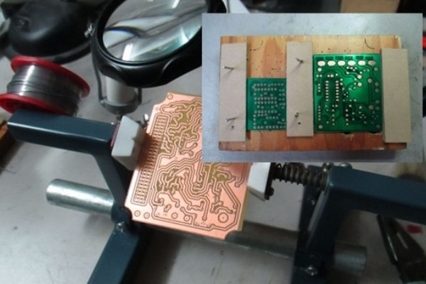
Using laser and iron printing, another method of making a printed circuit board
In addition, make sure that the design is printed as a mirror, because the default mode of most software when printing is on the option option. Another important point before transferring the image of the circuit is to completely clean the surface of the copper fiber with the help of dishwashing liquid, warm water and washing powder. Of course, to remove dirt on the fiber surface, you can go for fine sandpaper approximately 360. If the surface becomes dark after doing this, using a little lemon juice for cleaning seems like a good option and dry it at the end of the work. Remember not to touch the copper fiber after cleaning it so that you don’t face a problem during acid work due to greasy fiber.
Board ironing step in laser printing and ironing method
2- After the work surface is completely cleaned and polished, it will be time to place the glossy paper on which the circuit is printed upside down on the copper fiber. To do this, iron the iron with a high temperature until the paper takes on a slightly dark color and sticks to the fiber. Note that at this stage, the heat of the iron must reach all points uniformly, therefore, be sure to do this continuously; Also, be careful that ironing too much can cause the powder to spread and lead to the loss of the quality of the circuit. It can be said that considering about 10 minutes of ironing with high heat is enough to print a normal circuit. Of course, you will know the exact time by repeating the circuit print several times.
One of the signs of correct ironing that can be pointed out is a slight darkening of the color of the glossy paper attached to the fiber, as well as the appearance of the printed circuit design in a faint form from the side of the glossy paper. At this time, the temperature of the copper fiber is very high, so be careful with your hands when handling it.
3- In the next step, place the copper fiber in cold water, when the paper is pulpy and completely wet. Then by removing it from the water, separate the pieces of paper on it. At this stage, the complete and accurate transmission of the circuit design is done on the copper fiber.
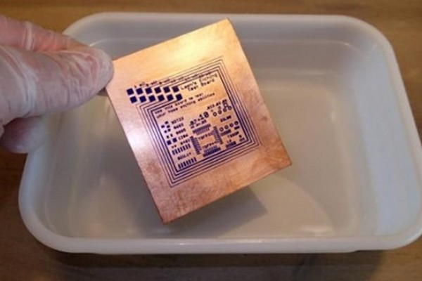
– Removing the extra copper sections from the printed circuit board will be the next step of this method. Usually, an acid called chloroferric, which is known as printed circuit acid in the market, is used to remove the copper parts without insulating coating. Perchlordoffer is available in the market in two forms, powder and crystal, and to use this acid, you must add some of it to hot water so that the resulting solution becomes colored tea. When working with this acid, you should only use non-metallic containers such as glass and plastic containers.
Then, after preparing the acid solution, put the printed circuit fiber in it and start shaking it slowly. Removal of excess copper parts is done after a short period of time, which you should continue until it is completely gone. If the fiber is placed in the acid in an inclined manner, the effect of the acid will increase, and in such a case, be careful that the fiber stays in the acid for 5-10 minutes. Because the acid enters the parts below the print and will cause the design to fail.
5- In the next step, after removing the copper fiber from the acidic solution, wash it with cold water and remove the remaining toners on the fiber with the help of a dishwashing wire.
Making a printed circuit board with the help of laser printing and heating device
This method is very similar to the method of using laser printing and iron in making printed circuit boards, and the only difference is that a heating device or card press is used instead of an iron.
Using positive spray 20
The positive spray method is suitable for student works. Positive 20 spray, caustic soda (sodium hydroxide) and transparent talc or film are some of the materials needed to perform this method of making a printed circuit board. First, prepare a positive 20 spray. Note that if the spray remains, it may be rotten. Its presence is high and it will not be sensitive to light. You can also go to a medical equipment store and buy it at a relatively cheap price.
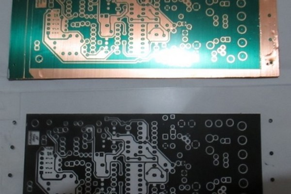
ساخت برد مدار چاپی به کمک چاپ لیزری و دستگاه حرارت دهنده
در ادامه این بخش از وبسایت پالس تک، روش ساخت برد مدار چاپی با این روش را شرح خواهیم داد.
۱- ابتدا به منظور پیاده سازی طرح برد مدار چاپی، به تهیه چند طلق ترانسپرنت که دارای قابلیت چاپ با پرینت لیزری است، بپردازید. رنگ نقاط و مسیری که باید بر اساس طرح، مس داشته باشد، مشکی بوده و سایر نقاط باید خالی باشد. سعی کنید، دو نسخه پرینت از طرح خود گرفته و با قرار دادن روی هم، مانع از عبور نور از جاهای چاپ شده شوید.
۲- سپس، برای رفع هرگونه چربی و کثیفی روی فیبر مسی، از یک سمباده نرم استفاده کنید.
۳- در این مرحله از ساخت برد مدار چاپی، بعد از اینکه فیبر کاملاً خشک و تمیز شد، سطح مس را با اسپری پوزیتیو که به شکل افقی و در فاصله ۳۰ سانتی و با زاویه ۴۵ درجه از فیبر گرفته اید، به صورت یکنواخت و با حرکت منظم دست بپوشانید. البته این کار را در مکانی دور از وزش باد و گرد و غبار و جای تاریک انجام دهید. در صورت پوشش کامل فیبر با یک بار اسپری زدن، دیگر نیاز به تکرار مجدد آن نمی باشد.
۴- پس از آن، اجازه دهید فیبر مسی به مدت ۲۴-۱۲ ساعت در جای تاریک باقی بماند تا خشک شود یا اینکه با گرم کردن این کار را انجام دهید. در صورت داشتن دستگاه خشک کن فیبر، می توانید به سراغ آن بروید. اما در غیر این صورت باید اقدام به حرارت دهی ملایم و به میزان ۷۰ درجه، روی یک اجاق و درون یک ظرف فلزی نمایید. ظرف مناسب انجام این کار می تواند یک قابلمه بزرگ باشد که به منظور جلوگیری از حرارت دادن مستقیم فیبر، گذاشتن چند تکه فلز بر روی کف آن ایده خوبی است. پس از ۱۵-۱۰ دقیقه فیبر به طور کامل خشک خواهد شد. یکی از نکات حائز اهمیت در این روش این است که کلیه مراحل باید در مکان تاریک اجرا شود.
۵- حال با تهیه یک ظرف بزرگ دیگر، دو تا سه لامپ معمولی یا یک لامپ مهتابی یا گازی کوچک را با توجه به سایز طرح درون آن قرار دهید. سپس با گذاشتن یک شیشه روی ظرف، فیلم یا طرح چاپ شده را روی آن جای دهید.
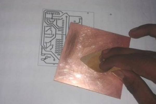
printed circuit board
6- After that, place the fiber so that the painted copper surface is facing down and on the printed design. Use a weight or another glass to weigh the fiber so that the fiber adheres to the design with high pressure during exposure. A dark place is needed to perform all these steps. Now, by turning on the moonlight or the lamp, light it for 20-30 minutes, and of course, this time depends on the intensity of the light and, most importantly, the quality of the spray you use. So, if the spray is fresh, this period can be less than this amount. Because in these conditions, you will see a faster reaction from the fiber exposed to light.
7- Now dissolve caustic soda with water in a container. Then, pour enough water in the container to cover one centimeter of the fiber and add approximately 10-20 grams of soda to it. If you use more than this amount of profit, it is possible to eat all the positive color. Now stir it to completely dissolve the soda in the water.
8- At this stage, put the copper fiber in the soda solution in an almost dark place and start shaking the solution very slowly for about 30-60 seconds. At this stage, you can dip some cotton in the caustic soda solution and gently rub it on the board. After a short time, you will see the voids slowly dissolve in the solution. Now quickly remove the fiber from the solution and wash it with water. Next, it is necessary to drop it into perchlorodofer acid solution.
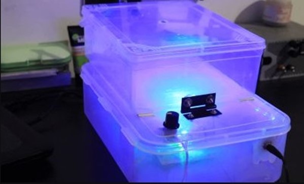
The method of making a printed circuit board
Making a printed circuit board with the help of laminate and UV rays
This method is suitable for very professional and precise work and is generally used in printed circuit board factories. In this method, the printed design of the negative circuit or transparent and laminate based on the desired cross section and also the acid of the printed circuit are needed.
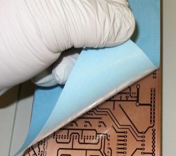
In relation to laminate, we must say that it is a light-sensitive plastic sheet with a small thickness and green or blue in color, which in fact uses a light-sensitive chemical substance between its two plastic sheets. The plastic cover on one side is elastic and soft, and the cover on the other side makes a sound when separated and has a thin sheet. We will witness the color change of the laminate with intense light radiation in a short period of time, which also changes its chemical properties. The printed circuit prepared with the help of this technique is very precise and clean and will not be different from the commercial samples of PCBs.
Description of the procedure:
1- First of all, you need to prepare a negative print of your design. First, draw the printed circuit diagram in a graphic program such as Photoshop, and then by comparing it, you should create your negative circuit diagram. Do not forget that the printed circuit map must be negative, that is, the place of the copper lines on it should be considered empty and the other places of the circuit should be black.
2- In the next step, try to remove any fat on the copper fiber using soft sandpaper or washing it.
3- Laying laminate on copper fiber can be considered the most important part of this method. After removing the softer laminate in half, place it on the fiber and, as you are removing the underside, proceed to glue the other side of the laminate over the fiber. Be careful not to create air bubbles under the laminate. If this happens, you should remove the air bubbles with a needle after gluing the laminate.
4- Now, in order to firmly stick the laminate on the fiber, stretch your hand over it for 5-10 minutes. To do this, in the industry, a heating device or card press with low heat is used. Ironing can also be a suitable option, but a wet cloth should be placed between the fiber and the iron and the iron should be set to a low level.
5- After finishing the work of making the printed circuit board, cut the extra laminates with a razor by reversing the fiber.
Using the UV device at this stage of making the printed circuit board
6- Then the laminate is exposed with the help of a UV device, which usually takes less than 1 minute. For this purpose, put the negative design on the device and then, by placing the fiber on which the laminate is placed, perform the exposure process. Do this for 1 minute.
7- Now, by removing a thin sheet on the laminate under soft light, prevent the unseen parts of the laminate from appearing.
8- At this stage, the emergence of the fiber is done. By doing this, the parts of the fiber that cannot be seen are separated. For emergence, you need to combine a tablespoon of emergence powder, which is baking soda or sodium bicarbonate, with some water. In other words, pour half a centimeter of water into a 20 x 10 cm container. Now put the fiber in it.
9- After 5-10 minutes, gently pull your hand on the fiber to separate the laminates that have not seen the light, and finally wash the fiber under water.
10- Now it’s time to acidify and remove the copper from the part of the printed circuit board that is not exposed to light. Don’t forget that the unexposed copper parts are completely dissolved in the acid and are clearly visible. But other parts under the blue laminates will not be soluble in acid. For acidification, mix a ratio of 1 to 2 high chlordopher acid in boiling water. Use a non-metallic container for this. Avoid pouring acid into water to prevent it from splashing in the eyes, and on the contrary, pour water slowly over the acid. Now by placing the fiber in the container, shake the container for 5-10 minutes to prepare the printed circuit board.
The step of removing the laminate from the board
11- then use sandpaper or a razor to remove the laminate from the copper parts of the printed circuit board; But the best way to do this is to use caustic soda. Pour a third of a tablespoon of soda into a container and add half a centimeter of water to it. 1-3 minutes of time is needed to separate the excess laminates according to the soda concentration. Now your fiber is ready for drilling and then assembling parts on it.
Of course, the type of laminate plays a role in whether the printed circuit board design is positive or negative. In general, we must say that to use this method, you need UV insulation, printed circuit fiber sensitive to positive or negative light, distilled water and a transparent sheet. Perhaps you can find a ready-made board, usually a black nylon sheet on it, and apply a special light-sensitive spray on one side of the fiber, which has a copper coating. In the next step, try to print the printed circuit board design on a transparent sheet. Then cover the copper surface with a transparent sheet on which the printed circuit board is placed and align it. Now put both of them in the UV insulation device for 15-20 minutes. Also, use PHOTOREVELATOR to remove extra parts. Finally, clean it with distilled water and place it in the acid container.
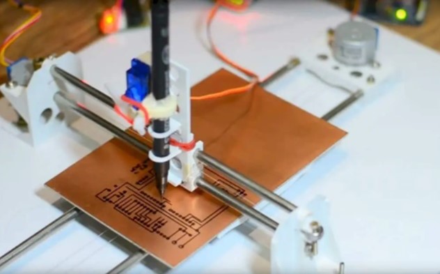
Making a printed circuit board with a CNC machine
Making a printed circuit board with a CNC machine
This method of making printed circuit board is suitable for producing printed circuit board with high circulation. This method does not require printing the design on copper fiber and also acid treatment. In this technique, after transferring the circuit PCB design to the computer of the CNC machine in the form of files with a special format, the machine will engrave the desired design on the copper fiber. Of course, the drilling process is done first and then engraving. Due to the expensiveness of this device, it will only be cost-effective to print a large number of printed circuit boards with it. It should be noted that the quality of the board obtained by this method is very high.
The printed circuit board is one of the most important electronic parts used in electrical devices and equipment. For the proper functioning of these devices, this very important piece plays the main and most important role despite being small. It is on this basis that making a printed circuit is considered one of the most important steps in making all kinds of electronic devices. Some of the other names for these boards can be mentioned below:
• Electronic board
• Printed circuit
PCB
• PCB board
The need for an expert in the manufacture of printed circuit boards
Some people think that anyone can make a printed circuit with a little simple training. Maybe this issue is true in relation to circuit printing in very simple and common types, but it will definitely not always be the answer for all types of electrical devices. Especially, these parts have many applications and a special design is needed for each type of application. For this reason, the best option is to have all the work steps done by experienced professionals.
Experts active in this field know all the details of the work due to the design and manufacture of various types of printed circuits. First, they easily identify the best type of printed circuit board needed by a device. After accurately identifying the requirements of a device, they design and manufacture it with the best possible quality. But exactly what type of electronic component is a printed circuit board?
High quality printed circuit board manufacturing
In order to make the printed circuit more clear, knowing the printed circuit board will be a great help in this field. Because by knowing the structure of these parts, what should be there to make these parts is better defined.
These electronic parts consist of one or more layers. Dozens and sometimes even hundreds of parts such as resistors, capacitors, ICs and other parts are placed on this screen. The printed circuit board connects all these parts in the best possible way and in the least space. As mentioned, the printed circuit board can be designed in very simple types or in extremely complex models. All these printed circuits generally have the following two parts:
bottom board
This thin board has a diameter of approximately 1.6 mm. The material of this part is generally chosen from resin and fiberglass. This board is mostly available in green color in the market, but there are also orange, blue and yellow colors.
Thin layer of copper
This layer is electrically conductive due to its copper material. If the thin copper layer is used on one surface of the printed circuit, it is called a single-sided printed circuit. If the copper layer is used on both parts of the printed circuit board, it is called a double-sided printed circuit board. The copper is placed in the printed form on the bottom board. Any parts that are necessary to give proper functioning of electrical devices are soldered on this board. This electronic board connects all these parts.
Applications of printed circuit
The importance of making a printed circuit becomes more clear when its different types are seen in all electrical devices. In fact, today’s modern devices will not work without these electronic parts. Some systems and devices that can only work with a printed circuit board include the following:
• Audio and music systems
• Air conditioning systems
• Microwave device
• TV remote control device
• Lighting tools
• Electric heater chambers
• Robotic vacuum cleaners
• Digital watches
• Home alarm devices
• CD players
• Home theaters
• Handheld video games
• Electric toys with remote control
• Television
• Computer
• Cellular phone
• washing machine
• Iron
Essential tips for manual printed circuit making
With all the explanations mentioned, people who are interested in making PCBs manually without using modern equipment for any reason should keep the following points in mind so that they don’t get into trouble:
Wear plastic gloves.
Place a newspaper or a suitable mat under your workplace so that your work floor is not damaged.
Dissolve 2 to 3 teaspoons of iron chloride in water.
Place the PCB in the etching solution (iron chloride solution, FeCl3) for approximately 30 minutes.
FeCl3 reacts with unmasked copper and removes unwanted copper from the PCB (this process is called etching).
Use the pliers to pull out the PCB and check if the entire uncoated area is etched. If it is not engraved, leave it in the solution for some time.
High quality printed circuit board manufacturing
Remember that only doing basic work can result in a device with good performance. In addition, to have devices that work in the best possible way for a long time, you need to print the circuit in a basic way; Therefore, choosing a collection like Pulse Tech, which has a long successful history in this field, is considered the best option.
Pulse Tech Group, having expert forces, can undertake zero to one hundred printed circuit design and manufacturing. Because the knowledge and experience of the employees are such that they perform all the steps at the highest possible level. In general, this company moves from providing all kinds of parts necessary for work to quality control according to the customer’s opinion. With this work policy, customers get exactly what they want. In addition, this company has made the entire work process easier for its customers by designing the printed circuit board online. In this way, the whole work is executed in a completely precise and calculated manner, as quickly as possible and with excellent quality.

بدون دیدگاه